2-4inch Gallium Nitride (GaN) Templates on Sapphire Substrates/silicon wafers
1. What is templates
We use the term "template" to describe our products as they are different to substrates. Specifically, a template is a composite or engineered substrate, where one or more layers are added to the original susbstrate.
2.Application
Blue and white LED for room lightings, displays and general use
GaN power switching devices
3.Product available
2" to 4" GaN-templates on FSS and PSS
Thick GaN-templates (t=3~20μm)
GaN-template with highly doped n-type layer (n=<1e19/cm3)
Ntype (undoped), Ntype (Si doped), and Ptype(Mg doped) templates are available
GaN Templates on both sapphire substres and Silicon substrates
4. Features
| XRD-FWHM | 002 | 102 |
| 3-4μm GaN/Sapphire | 200-300 | 250-450 |
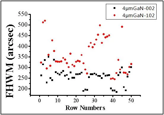
Dislocation density:3.5E+08 cm-2
5. Specification
2inch specification
| Item | GaN-FS-C-U-C50 | GaN-FS-C-N-C50 | GaN-FS-C-SI-C50 |
| Dimensions | Ф 50.8 mm ± 1 mm | ||
| Thickness | 350 ± 25 µm | ||
| Useable Surface Area | > 90% | ||
| Orientation | C-plane (0001) off angle toward M-Axis 0.35°± 0.15° | ||
| Orientation Flat | (1-100) ± 0.5°, 16.0 ± 1.0 mm | ||
| Secondary Orientation Flat | (11-20) ± 3°, 8.0 ± 1.0 mm | ||
| Total Thickness Variation | ≤ 15 µm | ||
| BOW | ≤ 20 µm | ||
| Conduction Type | N-type (Undoped) | N-type (Ge-doped) | Semi-Insulating (Fe-doped) |
| Resistivity(300K) | < 0.5 Ω·cm | < 0.05 Ω·cm | >106 Ω·cm |
| Dislocation Density | 1~9x105 cm-2 | 5x105 cm-2 ~3x106 cm-2 | 1~9x105 cm-2 |
| 1~3x106 cm-2 | 1~3x106 cm-2 | ||
| Polishing | Front Surface: Ra < 0.2 nm. Epi-ready polished Back Surface: Fine ground | ||
| Package | Packaged in a class 100 clean room environment, in single wafer containers, under a nitrogen atmosphere. | ||
4inch specification
| Item | GaN-T-C-U-C100 | GaN-T-C-N-C100 |
| Dimensions | Ф 100 mm ± 0.1 mm | |
| Thickness | 4 µm, 20 µm | |
| Orientation | C-plane(0001) ± 0.5° | |
| Conduction Type | N-type (Undoped) | N-type (Si-doped) |
| Resistivity 300K | < 0.5 Ω·cm | < 0.05 Ω·cm |
| Carrier Concentration | < 5x1017 cm-3 | > 1x1018 cm-3 |
| Mobility | ~ 300cm2/V·s | ~ 200 cm2/V·s |
| Dislocation Density | Less than 5x108 cm-2 | |
| Substrate structure | GaN on Sapphire(Standard: SSP Option: DSP) | |
| Useable Surface Area | > 90% | |
| Package | Packaged in a class 100 clean room environment, in cassettes of 25pcs or single wafer containers, under a nitrogen atmosphere. | |
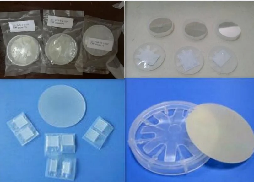
6. Product pictures
FAQ:
Q: What's the way of shipping and cost?
A:(1) We accept DHL, Fedex, TNT, UPS, EMS etc.
(2) If you have your own express account, it's great.If not,we could help you ship them.
Q: How to pay?
A: T/T, Paypal, etc
Q: What's your MOQ?
A: (1) For inventory, the MOQ is 5pcs.
(2) For customized products, the MOQ is 10pcs-25pcs.
Q: What's the delivery time?
A: (1) For the standard products
For inventory: the delivery is 5 workdays after you place the order.
For customized products: the delivery is 2 or 3 weeks after you place the order.
(2) For the special-shaped products, the delivery is 4 or 6 workweeks after you place the order.
Q: Do you have standard products?
A: Our standard products in stock.
Q: Can I customize the products based on my need?
A: Yes, we can customize the material, specifications and optical coating for your optical components based on your needs.